Frontiers of Engineered Coherent Matter and Systems: Proceedings of a Workshop (2025)
Chapter: 3 Solid-State Platforms
3
Solid-State Platforms
In the workshop’s second session, three presenters discussed various solid-state platforms for the study of engineered coherent matter and systems. The session, moderated by Prineha Narang of the University of California, Los Angeles, included the three presentations followed by a panel discussion carried out by the three panelists along with various audience members. The types of networks that can potentially be created from the systems discussed in this chapter differ from the networks that may be created from the systems discussed in the previous chapter.
NETWORKS OF QUBITS
Will Oliver of the Massachusetts Institute of Technology (MIT), who spoke virtually, described his work in emulating Bose–Hubbard models with arrays of superconducting qubits. He began with a brief overview of the different types of quantum simulation, ranging from natural materials to simulators. The experiments he would be talking about fall somewhere in the middle of that range, he said.
Specifically, he works with superconducting qubits, which serve as artificial atoms. The approach he uses is what he calls “analog/hybrid,” as opposed to a digital approach using a series of digital gates. “With analog/hybrid simulations, we’re basically setting or sweeping the Hamiltonian parameters continuously,” he said. “We may use some digital gates to initialize or benchmark—that’s the hybrid part. And as a result, we watch the system evolution unfold.” He referred to this approach as a quantum emulation of a system, as opposed to a quantum simulation. In an emulation, the system evolution mimics the Hamiltonian of interest; in
a simulation, the system evolution is encoded and inferred from an algorithm, he said, although people tend to use the terms almost interchangeably.
In his experiments, he used square arrays of 9 and 16 superconducting qubits, with XYZ controls for each site, which can be manipulated independently. The qubits can be coupled distinctly and uniquely with always-on and parametrically driven coupling. The readout is site resolved, simultaneous and unique, and the arrays are used to emulate the Bose–Hubbard Hamiltonian.
Oliver next provided some details on superconducting qubit arrays. Superconducting qubits are electrical circuits that are oscillators, he said, but they are nonlinear, and that nonlinearity comes from the Josephson junction, which is a nonlinear inductor. The Josephson junction in parallel with a capacitor forms a nonlinear oscillator at cryogenic temperatures. It has multiple discrete energy levels, and the bottom two energy levels, 0 and 1, are used in the qubit.
In building his arrays of artificial atoms, the building block that Oliver uses is a transmon qubit (Figure 3-1), which is a type of nonlinear oscillator that operates at cryogenic temperatures. Its Hamiltonian includes a simple harmonic oscillator term as well as a fourth-order nonlinear term.
Coupling two of these together via a capacitor creates what one can think of as an artificial molecule. The capacitance leads to an always-on coupling, but the resulting exchange interaction between the qubits happens only when those qubits are biased at the same frequency. If the qubits are detuned in frequency, even though there is a static coupling between them, the qubits do not exchange effectively. The Hamiltonian for this system includes two simple harmonic oscillator terms, one for each qubit, plus a coupling term with a strength J—referring to the exchange interaction between the qubits—and also some nonlinear higher-order terms.
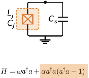
SOURCES: Will Oliver, Massachusetts Institute of Technology, presentation to the workshop, October 3, 2024, reprinted from P. Krantz, M. Kjaergaard, F. Yan, T.P. Orlando, S. Gustavsson, and W.D. Oliver, 2019, “A Quantum Engineer’s Guide to Superconducting Qubits,” Applied Physics Reviews 6(2):021318zz, with the permission of AIP Publishing.
To create a quantum emulation of a systems, such as a Bose–Hubbard model, Oliver’s team assembles these transmons into an array, generally 3 × 3 or 4 × 4 (Figure 3-2). One important detail, he said, is that instead of using a fixed-frequency transmon, his team splits the junction into a SQUID (superconducting quantum interference device). This creates two junctions, and if they put a magnetic field through that loop, they are able to tune the qubit’s frequency, which allows them to bring the various qubits on and off resonance with one another.
To realize the Bose–Hubbard model, Oliver’s team manufactures a chip with a 4 × 4 array of these tunable-frequency qubits which are capacitively coupled. The Bose–Hubbard model has a local site energy, which is the qubit frequency, and it also has an onsite interaction, which corresponds to the qubits’ anharmonicity, U, and a nearest-neighbor interaction (via capacitance), J. In their model, the local site energy (qubit frequency) is tunable and typically ranges between 3 and 5 GHz. U is on the order of 200 MHz, and J is 6 MHz. This transmon array emulates the Bose–Hubbard model in the hardcore limit, that is, when U is much larger than J, so the onsite interaction is much larger than nearest neighbor interaction strength. In particular, that implies that the second excited state is not excited.
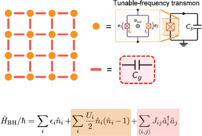
SOURCES: Will Oliver, Massachusetts Institute of Technology, presentation to the workshop, October 3, 2024, inspired by P. Krantz, M. Kjaergaard, F. Yan, T.P. Orlando, S. Gustavsson, and W.D. Oliver, “A Quantum Engineer’s Guide to Superconducting Qubits,” Applied Physics Reviews 6(2):021318zz and I.T. Rosen, S. Muschinske, C. Barrett, et al., 2024, “A Synthetic Magnetic Vector Potential in a 2D Superconducting Qubit Array,” Nature Physics 20:1881–1887.
Quantum Random Walks
Oliver then discussed a number of experiments that his group has carried out on these quantum arrays. He began with a brief description of quantum random walks, which were carried out on a 3 × 3 array. The group would create an excitation in the lower-left qubit on the array and let it “walk” through the array taking left and right turns randomly until it got to the upper right qubit, at which point it headed back to the origin, again taking random turns at each step, and the walk kept repeating back and forth over time. The experimental results mirrored the simulation quite closely, Oliver said.
Among the other experiments the team has carried out on 9- and 16-qubit chips are work with out-of-time-ordered correlation functions, studies of area versus volume law entanglement, and work with quantum attention networks. But for his presentation, Oliver focused on two particular examples more closely aligned with the topic of the workshop—work on Anderson and Stark localization with Bloch oscillations and on synthetic magnetic vector potential.
Localization Experiments
Because the energies of each qubit in an array can be tuned individually, Oliver said, his team can come up with statistical distributions of their disorder and vary that strength, creating different amounts of disorder in the array. Then, having set the amount of disorder, they can create an excitation and see how far it travels. When the level of disorder is low, he said, the travel is extensive, extending across the entire lattice. But as the disorder is increased, the excitations do not travel as far. This is a type of Anderson localization. The experimental data match both simulation and theory very well, Oliver said.
His team also varied that experiment by applying an effective electric field to the lattice and creating a Wannier–Stark ladder. “We do this by just shifting the energies with respect to one another of those qubits, say, linearly,” he said. Now when his team creates an excitation, say at qubit 2, it wants to spread out and go to qubits 1 and 3 and so forth, but because of the gradient of the electric field, the excitation returns back to qubit 2. This repeats, creating an oscillation, which is called a Bloch oscillation.
Flip Chip
Oliver next offered a few details on the chip they have developed to hold their 4 × 4 arrays of superconducting qubits. As they move from a 9-qubit chip to a 16-qubit chip, he said, the work of getting the wires into the qubits got more challenging, and over time they developed a number of technologies to deal with the
additional complexity. In particular, he described their flip chip design, which uses a standard approach in semiconductor manufacturing for connecting the devices on a chip to external circuits.
Moving to the flip chip technology not only dealt effectively with the challenges of wiring the qubits, but it also lowered the calibration requirements for the chip, Oliver said. One challenge with the arrays of superconducting qubits, he explained, is that there tends to be quite a bit of crosstalk among the qubits in addition to the desired communication between a control qubit and a response qubit, requiring calibration. However, he said, moving to the flip chip “added some screening, and it also added some design flexibility that allowed us to improve this situation dramatically.” Using the flip chip decreased the crosstalk by a factor greater than 10, and the flip chip’s design flexibility allowed them to decrease the crosstalk by another factor of 5. With the flip chip, the cross talk is now somewhere between 0.1 and 1 percent.
Oliver then provided some specifications for the 4 × 4 flip chip. Its excitation frequency is around 4.5 GHz, its average anharmonicity is −218 MHz, and its average T1 is 22.8 μsec. The average readout fidelity is 93 percent, and the average randomized benchmarking fidelity is 99.8 percent for individual qubits and 99.6 percent for simultaneous qubits.
Synthetic Magnetic Vector Potential
There are many examples of physics that one would want to emulate that require magnetic fields, such as quantized Hall states, topological superconductivity, the Hall effect, weak localization, and the anomalous Hall effect. However, while in typical condensed matter experiments it is relatively straightforward to carry out experiments in the presence of a magnetic field by putting the experimental apparatus inside a large magnet, it is not so easy with experiments on quantum arrays. In particular, Oliver’s team biases and tunes their superconducting qubits using a biased magnetic field, and if they attempted to emulate a system in the presence of an external magnetic field, it would destroy the qubits. So the team developed a way to make a synthetic magnetic field that would allow them to carry out emulations with their biased magnetic field tuning the qubits.
Emulating a magnetic vector potential is the starting point, Oliver said, and he went into some detail on how one accomplishes that in an array of superconducting qubits. In essence, it is done with a Peierls substitution (Figure 3-3). In a continuum model, he explained, the kinetic energy term of the Hamiltonian has a vector potential, but in the discrete case, one can make a Peierls substitution so that in a lattice model, neighboring qubits or neighboring lattice sites, m and m + 1, have a coupling strength between them, but a Peierls phase also shows up.
When the neighboring qubits are in resonance with each other, there is a direct transverse coupling between them, and they will exchange energy back and forth

SOURCES: Will Oliver, Massachusetts Institute of Technology, presentation to the workshop, October 3, 2024, inspired by P. Krantz, M. Kjaergaard, F. Yan, T.P. Orlando, S. Gustavsson, and W.D. Oliver, “A Quantum Engineer’s Guide to Superconducting Qubits,” Applied Physics Reviews 6(2):021318zz and I.T. Rosen, S. Muschinske, C. Barrett, et al., 2024, “A Synthetic Magnetic Vector Potential in a 2D Superconducting Qubit Array,” Nature Physics 20:1881–1887.
with a strength J; if the qubits are detuned, that direct transverse coupling turns off. “However,” Oliver said, “if we now drive that transition parametrically at the difference frequency between those qubits, we can create this Peierls phase. We can turn on the coupling J, which is a function of the strength of our driving, the amplitude of the field that we’re using to drive this parametrically, and by the choice of the phase we use in the drive, we can actually implement that Peierls phase.” The bottom line is that one can set the Peierls phases in the lattice by parametrically driving pairs of superconducting qubits, thereby emulating the magnetic vector potential. Importantly, it is possible to do this simultaneously on all pairs of qubits.
Oliver then offered a number of examples of the sorts of experiments that can be done on the arrays of superconducting qubits with such a synthetic magnetic vector potential added. In the first, carried out in a square of 4 qubits, he demonstrated the effects of turning on the synthetic magnetic vector potential by applying a Peierls phase of π between 2 qubits. Without the synthetic magnetic vector potential, an excitation would travel back and forth through a random quantum walk among all 4 qubits, but once the Peierls phase was applied, the excitation was restricted from traveling to one of the qubits—a case of Aharonov−Bohm caging. Oliver emphasized that the team is able to make measurements on all of the superconducting qubits simultaneously and map out what is happening at each one, not just the first one and the last one. And they have seen the Aharonov−Bohm in rings of 8 and 12 qubits, with the experimental results matching up well with the simulation and the model each time.
The team was also able to do a test of gauge invariance for the synthetic magnetic field. In essence, they tested whether the flux through a loop was equal to the oriented sum of the phases around the loop, and they found that indeed it was for a variety of conditions.
The presence of a synthetic magnetic field implies, through duality, that there should also be a synthetic electric field, Oliver noted, and its presence was demonstrated by the creation of Bloch oscillations. In particular, excitations traveling along a one-dimensional chain of qubits were restricted in their travel by a synthetic electric gradient, leading to the oscillations.
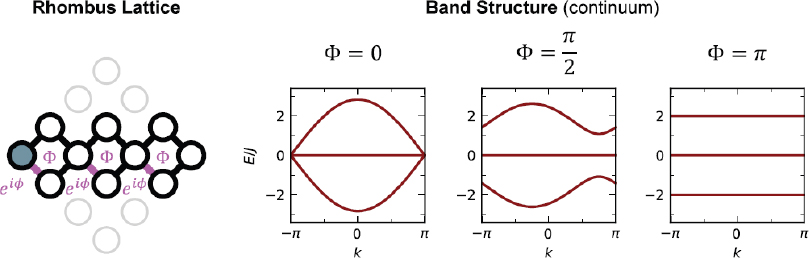
Finally, Oliver described how his team used the synthetic magnetic vector potential to emulate flat bands in one dimension. They strung together 2 × 2 plaquettes to emulate three-unit cells of the rhombus lattice, which always features one flat band in its band structure (Figure 3-4). The band structure depends on the Peierls phases, and if the flux through the loop is anything other than π, there will be only one flat band, but at the phase π, there are three flat bands.
The flat bands lead to localization, Oliver said. Looking at RMS position, which he described as a ballistic transport and a proxy for conductivity, one finds that it drops to almost zero in the flat band limit—in other words, when the flux approaches π. The localization length is also minimized at the flat band condition, he continued, so the particle motion is basically arrested near the flat band condition and velocity goes to zero.
Oliver’s last observation was that Anderson localization is reversed near the flat band condition. When the flux is zero, Anderson localization holds, with localization increasing as disorder increases. However, when the flux is π, increasing disorder leads to delocalization.
In response to a question from an audience member about how large an array his team will be able to create and how the fidelity will change as they go to a larger system, Oliver said that the next step will be go to 25 qubits, but “as an academic institution, our goal is not necessarily to just go to as many qubits as possible, but
SOURCES: Will Oliver, Massachusetts Institute of Technology, presentation to the workshop, October 3, 2024, adapted from I.T. Rosen, S. Muschinske, W.D. Oliver, et al., 2024, “Flat-Band (De)Localization Emulated with a Superconducting Qubit Array,” arXiv preprint, https://doi.org/10.48550/arXiv.2410.07878.
rather to understand, in some sense, how to scale.” They leave it to large corporations such as Google or IBM to actually do that scaling, he said, noting that such companies have built systems with 100 qubits or more with very high fidelities. “Our goal is really to do good science, good engineering, understand how to scale, and then publish those results so that we can help our partners in industry do that scaling.”
USING NITROGEN–VACANCY CENTERS TO PROBE SUPERCONDUCTIVITY
Chris Laumann, an associate professor of physics at Boston University, spoke about the use of nitrogen–vacancy (NV) centers in diamonds as a tool for probing the properties of superconductors in diamond anvil cells. He commented that his talk would include much about quantum materials, it would have very little to do with networks. “The network topology involved is totally disconnected between the qubit elements,” he said, adding that he would touch on quantum networks a bit at the end of his talk.
As background, Laumann described the ongoing controversy about hydride superconductors. It began with a 1968 paper by Neil Ashcroft in which he predicted that if hydrogen could be placed under enough pressure that it became a metallic solid, then that solid form of hydrogen would be a superconductor at relatively high temperatures. Intuitively it made sense because the critical temperature of a superconductor is proportional to the characteristic frequency of the phonons (the Debye frequency) of the materials and also increases with the electron–phonon coupling; since both of these are large thanks to the very large mass of the hydrogen atom, the critical temperature should be high.
The problem, Laumann continued, is that hydrogen atoms bond strongly to create H2 molecules, and what happens when hydrogen is put under very high pressures is that it solidifies into a crystalline structure made up of the H2 molecules, which do not give up their electrons. Recent work on the phase diagram of hydrogen has indicated what the various phases of hydrogen should be at different temperatures and pressures up to well over 500 GPa, and no superconducting phases have been found (Pickard and Needs 2007). “Even metallicity is still controversial,” Laumann added.
After nearly four decades with no verification of his prediction, in 2004, Ashcroft updated it. Now he hypothesized that if hydrogen was combined with metal atoms, the metal would bind the hydrogen into some type of structure which would break the H2 bonds, thus getting to a metal more readily but still with the benefit of the hydrogen’s low-mass phonons. So Ashcroft suggested exploring hydrogen-dominant metallic alloys.
That prediction was “spectacularly realized,” Laumann said, although not in exactly the same materials that Ashcroft had predicted but in the same general class.
In particular, sulfur hydride, H3S, was found to be super conducting above 200 K and above 100 GPa (Drozdov et al. 2015). That discovery ushered in what Laumann termed “age of hydride high-Tc superconductors.” Many more of these materials have been reported in the past 10 years, he continued, although controversy has surrounded some of them, and some were later retracted.
The reason for the controversy and the retractions, he said, is that the experiments needed to verify superconductivity in such materials are notoriously difficult to perform for several reasons. First, to achieve the necessary pressures for these materials to become superconducting, they must be placed in diamond anvil cells (Figure 3-5). Such a cell is made with two flat-faced diamonds facing each other with a sample held between them in a volume that is contained by an insulated gasket; the diamonds are pressed together, and because the faces of the diamonds are very small and pressure is equal to force over area, one can exert very high pressures on a sample. It is possible to get to 100 or even 200 GPa with just some screws, Laumann said. With these pressures, the hydrides of interest can be created inside the diamond anvil cell, but they are not stable and will transform into a different phase if removed from the cell. Thus, they must be measured inside the cell.
However, making the necessary measurements inside a diamond anvil cell is not easy. Ideally, one would want to see two things happen to be sure that a material has entered a superconducting state. First, its electric resistance should go to zero so

SOURCE: Chris Laumann, Boston University, presentation to the workshop, October 3, 2024.
that electrical currents could flow without losing energy. Second, it should become diamagnetic, or exhibit the Meissner effect, meaning that it will expel magnetic flux. The first measurement is difficult to do in a diamond anvil cell, but still quite possible—one gets electrodes to come in under the gasket of this diamond, make contact with the same, and do a four-terminal measurement.
Until recently, Laumann continued, the main way to measure the magnetism in a sample and see if it exhibits the Meissner effect was to put the same material inside a conductive kind of coil and do a pickup measurement. However, since a diamond anvil cell is very small and is at a very high pressure, it is impossible to put a coil inside the cell, and if you put the coil around the entire apparatus, any magnetic signal from the sample tends to be drowned out by the magnetic signals from everything else. Furthermore, he continued, there are conflicts that arise between putting the leads into a cell to measure the resistance and having a coil around the cell. “Just geometrically, it’s hard to do the magnetic measurement if you also have leads going in,” he said.
One obvious approach, then, would be to do multiple samples, measuring the resistance in some and the diamagnetism in others. But various things can cause the resistance to drop in a sample, and the definitive indication of superconductivity is when one observes the electrical resistance transition at the same time as the diamagnetic transition, implying that the two measurement changes are resulting from the same phenomenon.
To address these issues, a group at the University of California, Berkeley, came up with an approach that used NV centers embedded into one of the diamonds in the diamond anvil cell. In particular, they embedded a shallow layer of NV centers about 50 nm below the sample-facing face of one of the diamonds. This made it possible to image the magnetic response of the sample locally and be able to see what is superconducting inside the system and to do it in a way that is compatible with making electrical resistance measurements at the same time.
Providing some background on NV centers, Laumann said that an NV center is a substitutional defect in a diamond created when two adjacent carbon atoms in a diamond are replaced by a nitrogen atom and a vacancy. “It is one of many, many, many stable color centers or defects which you can find in diamond,” he said, as researchers have used these in a wide variety of studies. In particular, he added, “it has been a workhorse for a long time in quantum sensing and quantum information.” For use in measuring magnetic fields in a diamond anvil cell, the key features of NV centers is that they are sensitive to local magnetic fields, which are controlled and read out optically, and they operate in a wide range of temperatures (from millikelvin to hundreds of degrees Kelvin) and pressures (from ambient pressure to at least 170 GPa).
One can think of an NV center as an artificial atom that has two electrons in its ground state that form a spin-one triplet, Laumann explained. There is also a
natural quantization axis, which is the axis from the nitrogen atom to the vacancy. There are three spin states: +1, 0, and −1. The environment of the surrounding diamond crystal splits the ±1 states from the zero state, which is at a lower energy.
The NV is called a color center because it fluoresces. If one applies green light, the vacancy will fluoresce red light back, and the more green light that is applied, the more red light will be emitted. When the NV center is in the zero-spin state, the red light will be a bit brighter than if it is in the +1 or −1 state, which makes it possible to tell which spin state the NV center is in. Furthermore, if one keeps shining green light on the diamond, it drives the NV center into the zero-spin state, so as long as nothing else is going on, one will always see the brighter amount of red light emitted, indicating the zero-spin state.
This makes it possible to use some classic electron paramagnetic resonance (EPR) techniques to probe things, Laumann said. One applies a microwave field to the NV centers and sweeps the microwave frequency until it hits a resonance with the transitions between the zero and ±1 states, driving the system out of the zero state toward the +1 or −1 state, making red light darker. The technique is called optically detected magnetic resonance (ODMR), and the product is known as an ODMR spectrum.
This can be used to detect a magnetic field because in the presence of a magnetic field the +1 and −1 states will split and have different energies. “So I can simply read out the magnetic field from the spacing between the peaks I see in this spectrum,” Laumann said. He uses a confocal microscope to examine the distribution of the red light being emitted by the NV centers, which will vary according to whatever magnetic field is being applied and thus can be used to detect the magnetic properties of a sample in the diamond anvil cell.
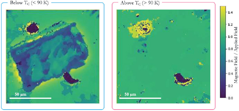
In particular, if a magnetic field is applied and the material in the sample is normal—that is, not superconducting, then the magnetic field that a researcher observes with the NV centers should match the magnetic field that is being applied. However, if the sample is superconducting, then it will expel magnetic fields, and the magnetic fields across the nearby NV centers will be suppressed. Laumann illustrated how this works by showing two images created from a sample of the superconductor bismuth strontium calcium copper oxide (BSCCO) in a diamond anvil cell when the BSCCO was below or above its critical temperature (Figure 3-6).
Doing the same thing with a hydride is more complicated than with BSCCO because, among other things, the hydride must be synthesized at pressure inside the cell. So, for instance, one puts a cerium flake in the cell, adds a bath of ammonia borane (CH3BH3), and then uses a laser to heat up spots around the edges of the cerium to about 1,500 K at 140 GPa. With luck, cerium hydride (CeH9) will form around the edges of the cerium where it has been laser heated.
Laumann then showed some images of a CeH9 sample from inside a diamond anvil cell using NV centers as a sensor which were exposed to an 80 Gauss (G) magnetic field. When the temperature in the cell dropped below about 90 K, the measured
SOURCE: Chris Laumann, Boston University, presentation to the workshop, October 3, 2024.
magnetic field was only 50 G, indicating a Meissner effect within the sample. At the same temperature, the resistance dropped sharply as well. Thus, at 140 GPa, CeH9 becomes superconducting at a critical temperature of around 90 K.
In particular, this nano-scale quantum sensing made it possible to do local sensing and determine details about CeH9 that could not have been seen before. In particular, Laumann said, it is clear that the synthesis of CeH9 is “synthesis is not that great.” It produces superconducting grains of around 5–10 microns, and not all of the laser-heated regions are superconducting. Nobody could have determined that before, he said. “Until you could look like this with the NV sensor, there’s no way to know.”
Looking to the future, Laumann said that he hopes this technique will help put to rest much of the controversy around the field of hydrides, but it will require going back and checking all of the hydrides that have been reported as superconducting to get more definitive data. For instance, he showed some month-old preliminary data on lanthanum hydride (LaH10) that indicated that the material is indeed superconducting at 170 GPa with a critical temperature of around 200 K, which is very high. “In the longer run,” he continued, “we would like to be able to loop that local imaging back into improving the synthesis and eventually be able to more generally use these NV-sensing techniques, even at high pressure, to correlate structural stress [and other] local information to improve material synthesis of all kinds of things.”
In closing, Laumann briefly described some other work from his laboratory that he said was closer to the specific topic of the workshop—that is, coherent
quantum systems. Those experiments are studying how hydrodynamics emerges from many NVs (or nitrogen spins) interacting at very low temperatures. “We think that the dynamics involved is actually the coherent dynamics of those spins, rather than something thermal coming from the lattice decohering it,” he said.
QUANTUM STATES IN SEMICONDUCTORS
David Awschalom, the Liew Family Professor of Molecular Engineering and vice dean for research and infrastructure at the University of Chicago’s Pritzker School of Molecular Engineering, spoke about developing semiconductor qubits for communication and sensing, controlling and extending the spin coherence of NV centers, and also using chemistry to mimic what has been done in solid-state systems to engineer tunable, portable, scalable qubits. “These are really new directions,” he said, “and it’s really fun to share them with you.”
As context, he said that the overall goal was to take advantage of the tremendous amount of technological development that has gone into semiconductors and use it for quantum applications. Conventional semiconductors operate by manipulating electric charges, whereas coherent spin electronics would be based on the direction of carrier spin and on spin coupling. The fact that the spin naturally couples to photons, phonons, and magnons would make it possible to create multi-functional interfaces and to both manipulate quantum information and also transform it, allowing the integration of memory, logic, and communication technologies into a single platform. “That’s a big goal, and it’s going to take a while to get there,” Awschalom said, “but things have gone really well in interesting ways in the last few years, and that’s what I’d like to talk about.”
Creating, controlling, and combining qubits in semiconductors involves overcoming many hurdles, he said. “How you create single quantum states in a broad platform is challenging,” he said, as is designing a more complex system to control the photonics, the electronic properties, the mechanics, and the magnotics, and he mentioned specifically using coherent magnotics to entangle quantum states. He then went into detail on some of the work that has been done to this end.
He began by briefly talking about manipulating and measuring spin qubits, using the NV centers in diamond that Laumann had discussed as his first example. The takeaway message, he said, is that an NV center is essentially a trapped atom in a semiconductor that you tune with magnetic fields. When a pulse of unpolarized light of resonant frequency hits the system, it “generates a spin polarized electron, often a spin 1 state, and that spin 1 state can be manipulated with microwaves.” As Laumann discussed, much has been learned about this system through years of experimentation.
About 10 years ago, Awschalom said, his group realized that it was unlikely that diamond is the only material that exhibits these properties, so they went looking
for others. “We did essentially a material screening calculation, a type of genetic screening,” he said. “So imagine you have a tetragonal lattice [like diamond has]. You create a defect. What other material would generate an energy diagram that looks like the one I just showed you?” To find out, his team carried out density functional theory calculations to screen a large number of materials and discovered several that they predicted would behave like diamond with NV centers. At the time, he said, they had difficulty publishing their results “because there was a lot of disbelief.”
One of the materials that popped up in their calculations was silicon carbide, which is used today in a wide variety of applications. It came as a surprise, Awschalom said, that a material that can be bought online would have an energy diagram that looks like the energy diagram of an NV center. And, he added, not only can it be easily bought online, but it is orders of magnitude less expensive that the diamond used in work on NV centers. Furthermore, silicon carbide can be doped to create n and p types, it can be grown on silicon, and it can be used to make various types of semiconductor devices. “It’s very popular in space technologies and avionics,” he said, “as basically silicon that works at high temperature.” Another advantage is that if one made silicon carbide qubits analogous to the NV center qubits in diamond, the silicon carbide qubits would emit photons at near telecom wavelengths, so they could easily be built into networks.
As an example of the sorts of quantum properties that can be built into silicon carbide, Awschalom showed data on quantum spin states taken from a single electron in a commercial 4-inch silicon carbide wafer. The data, which took about 15 minutes to acquire, had an excellent signal-to-noise ratio. “You can then use a Landau–Zener interaction and exchange that spin with a local nucleus—in this case, silicon 29—and develop a one-nuclear-spin memory with a longer lifetime,” he continued. “And you can entangle it too to make a quantum register.” The example illustrates, he said, “how much our knowledge has increased in this world—to be able to extract single quantum state dynamics in a commercial platform.”
Since such quantum states can be produced in silicon carbide, the obvious next step is to build the quantum state in a device. Such a thing would be very difficult to do with a platform like diamond, he noted, because one needs to make a p-n junction. “So we did the simplest thing,” he said. “We just bought a diode, a p-n junction, and implanted some defects in it to make quantum states, … apply the voltage, and began to look at the energies of the emission.” The device (illustrated in Figure 3-7, lower left) was far from optimized. “It’s 10-micron-layer silicon carbide, so it’s pretty big,” he said, but with it one could tune more than 800 GHz in quantum frequencies.
It may not be immediately obvious why this is a big deal, he continued, but with the line width that comes out of these quantum states, which is about 20 MHz, it would be possible to have tens of thousands of quantum channels
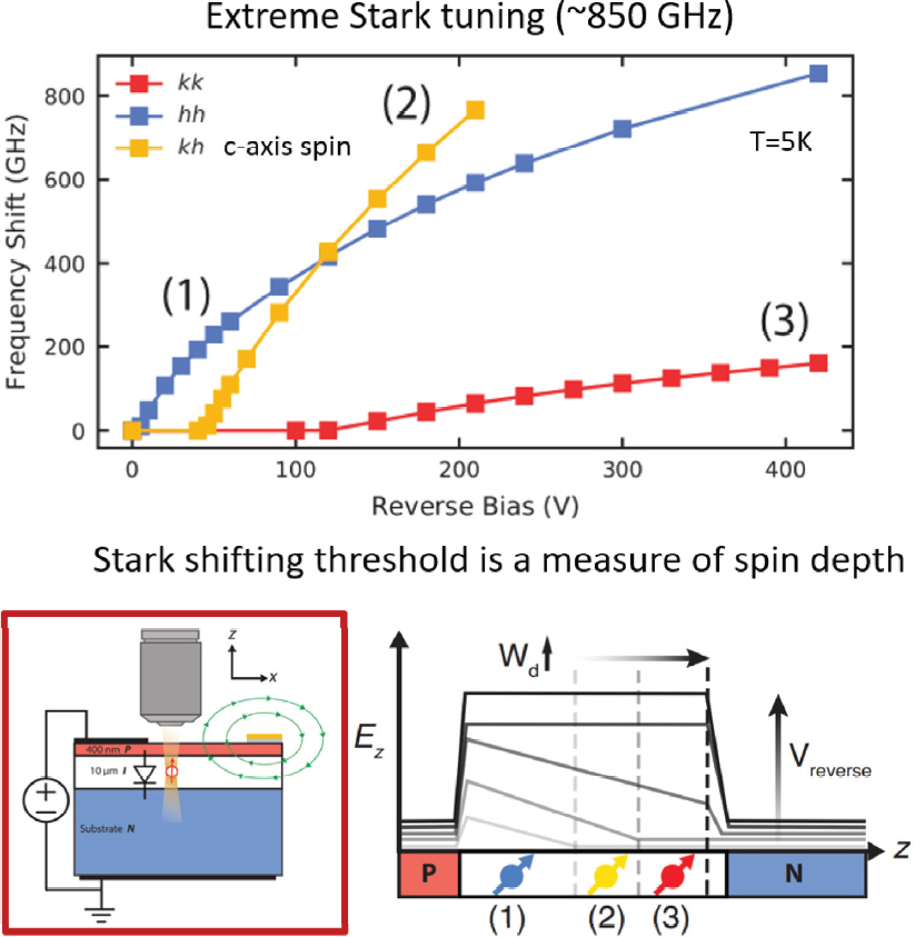
SOURCE: David Awschalom, University of Chicago, presentation to the workshop, October 3, 2024, from C.P. Anderson, A. Bourassa, D.D. Awschalom, et al., 2019, “Electrical and Optical Control of Single Spins Integrated in Scalable Semiconductor Devices,” Science 366(6470):1225–1230. https://doi.org/10.1126/science.aax9406. Reprinted with permission from AAAS.
in one fiber. This is possible because one can tune the quantum states based on electrical gain.
One of the surprises they found when testing the device was its stability, he added. A challenge with NV centers is that periodically an electron will hop out of the site, but that does not happen in silicon carbide, he said, for reasons that are
still not understood. Instead, the electron will just sit there for hours, and one can gate the optical transition on and off to make a single-photon source.
Next, Awschalom described engineering coherence in these platforms. Maintaining coherence over relatively long periods can be very valuable, he noted, particularly for use in memories. Nuclear spins in the solid-state host cause dephasing, and engineering the matrix and periodically driving the quantum state can increase coherence. To see how just far coherence could be pushed, Awschalom’s group collaborated with a group in Sweden that grew isotopically pure silicon carbide, and they used dynamic decoupling to mitigate the random nuclei that were left in the material. This pushed the coherence time to over 5 s at 10 K. This is a “pretty nice lifetime,” he commented; given that it takes a few picoseconds to flip a spin for an operation, “that gives you about 12 orders of magnitude of operational time within the lifetime.”
He spoke briefly about work his group did with vanadium atoms implanted into silicon carbide. Vanadium produces light at the telecom O-band1 frequency for communication, or at 1.3 microns. The vanadium defects in the silicon carbide produced single photons in the O-band, but different isotopes of vanadium produced photons with slightly different frequencies; that is, he elaborated, the optical emissions from these states can resolve a single additional neutron in an atom, and each neutron produces a 20 GHz energy shift. This material could conceivably be used as a neutron detector and also as a way to look at strain at the atomic level since the strain shifts these nuclear states and isotopic interactions. His point, he said, is that these materials offer a very rich scientific platform for using the coherence of quantum systems to look at related phenomena at the atomic scale.
More recently, in the same system, by taking the temperature down to 20 mK and looking at how the symmetry of the host changes the coherent properties, Awschalom’s team found that the spin relaxation time (T1) could now go down to half a minute, and changing the symmetry to cubic symmetry could drop it even farther, down 200 ms for the same qubit. “So again,” he commented, “it’s giving us scientific insight into how you engineer the host of a quantum state—not the state itself, but the environment of the state—to control the coherent properties.”
Switching from silicon carbine to other semiconductors that can be used in these quantum applications, Awschalom spoke about cerium oxide (CeO2), which had been identified as a candidate in calculations performed by students in Awschalom’s group as well as some Japanese collaborators. Cerium oxide has the advantage that it has basically no nuclear spin, so it is not necessary to isotopically purify it. Furthermore, by putting erbium into the cerium oxide, one ends up with a material that emits at the prime telecom frequency for networks, 1.5 microns. An additional advantage is that it grows on silicon; recent work showed that it is possible to get beautiful single crystals of cerium oxide doped with erbium grown
___________________
1 The original band (O-band) ranges from 1260–1360 nm.
on commercial silicon wafers. The material is also piezoelectric, allowing for on-chip tuning, and T1 values are in the millisecond range. “It’s not a great first set of materials,” he said, “but it’s working. So we’re pretty excited.”
Next, Awschalom discussed using a chemical approach to go to a smaller scale for these quantum materials. Paul Alivisatos at the University of Chicago used nanocrystal chemical synthesis to make cerium dioxide nanocrystals doped with erbium. The well-formed crystals were about 7 nm across. Crystals of this size make it possible to study various aspects of the qubits formed by the defects. One can, for instance, study the effect of the size of the host environment on targeted spin qubit performance, and the small size of the crystals allow researchers to study how the surface and the qubit interact. Furthermore, Awschalom added, these are very inexpensive and very flexible systems to fabricate.
His team made an unexpected observation concerning these nanocrystals, he added. The nanocrystals have organic ligands attached to their surfaces, and the spins of the erbium atoms in a crystal are coupled to hydrogen atoms on the ligands. The researchers did not shield the nanocrystals from Earth’s magnetic field, and they observed the erbium qubits in the nanocrystals “beating” because of the coupling with the hydrogen atoms in the presence of the magnetic field. These crystals also offer a “wonderful laboratory to change the erbium density, change the distance of the surface, and look at the [coherence] lifetimes,” he said. “It’s a pretty exciting direction, and we’re learning a lot from this,” he said.
Finally, Awschalom spoke about what he called a bottom-up approach to designing qubits. The idea is to design a qubit with atomic precision using theoretical molecular chemistry. It took years of trying, but eventually Danna Freedman, who was at Northwestern University at the time and now is at MIT, accomplished it by putting chromium in a dimethylphenyl group structure. For the first time, Awschalom said, researchers are now able to carry out atomic-scale engineering of a qubit environment. To illustrate, he showed three molecule structures that had the same qubit in the middle and whose only structural difference was the placement of a single methyl group; the three structures had very different quantum energies: 1.8 GHz, 3 GHz, and 4 GHz. “It means you can tune the quantum energies,” he said.
In summarizing, he said he had discussed now two basic approaches to creating and controlling qubits. The top-down approach is used in a variety of systems, including diamonds, silicon carbide, and oxides. Suppressing noise and engineering symmetry can extend coherence. Electrical control enables scalability and tuning over nearly terahertz frequencies, while using transition metal ion qubits makes it possible to operate at telecom frequencies.
In the bottom-up approach, there are emerging opportunities for creating molecular qubits. By taking advantage of a century of advances in chemistry, it is
possible to build analogs of semiconductor qubits but with atomic precision for functionalized targets of applications.
In response to a question about whether elements other than erbium might be useful in creating materials for telecommunications, Awschalom said that there are probably other rare earths that could work as well. The main reason he focused on erbium, be said, is because of work coming out of Princeton University showing that the erbium material had relatively long lifetimes at a frequency that was perfect for telecommunications, but his group is planning to look at other materials that have recently emerged.
James Thompson from JILA referred to Awschalom’s mention of interfacing his molecular systems with superconducting systems and asked, “Is your vision that this would be an ensemble coupling, or are you thinking single molecules coupled to superconducting circuits?” Awschalom answered that his team had been thinking a lot about that issue and at the moment is considering both. “One of the nice things with these molecular systems is that each of the qubits is exactly the same,” he said. “So it seemed to us that ensembles would be pretty interesting, because, essentially, it’s an array of atoms.” He had naively thought, he said, that a single molecule would offer a good approach, “but then the coupling coefficients seemed to be an issue with the superconducting qubits.” His team has been thinking about both.
DISCUSSION
Narang began the panel discussion by noting that, with the exception of Awschalom’s talk, most of the platforms that had been discussed to that point were not designed for use in telecommunications and then asking how important is it that these various networks operate in telecommunications frequencies. “I think it is pretty important to operate in the telecom frequency,” Awschalom answered, and even without repeaters, which may take some time to evolve, he suggested it should be possible to build very powerful networks at metropolitan scales that would cover large fractions of users in populations with existing fibers. Oliver agreed. “We know that we need to connect different quantum computing or quantum sensing nodes, or even quantum sensing to quantum computing nodes in the future,” he said. “And even though we’re still trying to build individual nodes at this point, we shouldn’t forget that we do want to do that connection in the future, so it’s a good idea to start thinking about and prototyping how we’re actually going to do that.”
Awschalom added that there is a practical aspect to this that people should be thinking about now—that is, the sheer size of the network that would be needed. Consider, he said, the number of cell phone towers needed to cover just Long Island. “The numbers are staggering.” Oliver suggested that a metropolitan-size network might be run like the current cable TV networks, where fiber optic cables
carry the signal most of the way to a destination, but the last segment is through a coaxial cable into a house.
Pedram Roushan of Google suggested that, practically speaking, there may not be much choice about the frequencies for the coming quantum networks because of technological lock-in of the choices already made. “There was some thinking originally that probably we can use off-the-shelf component to drive the qubits,” he said, “and it grew to a very large industry now that it’s just hard to shift away from.” Oliver added that the interfaces between the different quantum technologies are going to be critical because so many of them are being developed in parallel in such a way that they are not necessarily compatible out of the box with one another. “A good part of the engineering problem is going to be developing a good interface where, say, optical communication can effectively interface with an existing microwave-based technology.” Awschalom agreed and said that one of the great failures of fiber optic technology was that while an extraordinary amount of money was spent to deploy fibers all over the United States, there was nothing in the home to plug the fibers into that would take full advantage of the optical signal.
An audience member asked Awschalom if it might be possible to “tag” individual qubits in a group of them so that they could be tracked. Awschalom said that it is a question many people are thinking about. One could imagine, he said, applying a gradient magnetic field or gradient electric field to an array of qubits so that one could distinguish small ensembles of qubits, if not actually an individual qubit. There is not yet a proof of concept, though, he added.
Next, Narang asked the panelists how the platforms they had been discussing might be put to use carrying out work in fundamental physics. Laumann said that researchers working with NV ensembles have been thinking about how to engineer their interactions and go to low temperatures to study their intrinsic dynamics. “So then you do start asking questions, which come back to fundamental physics,” he said. “How do long-wavelength phenomena come out of these microscopic things? … Do you actually need entanglement to describe anything going on in the observables that you can measure?” A practical problem of going to low temperatures, he added, is that the experiments get really slow, and running them becomes a question of how long a graduate student will be willing to work on a single experiment.
Charlie Marcus asked Awschalom which technologies on the spectrum from atoms to solid-state materials might be best for applications in the future, particularly with respect to the operating times and coherence times of the various options. Awschalom said that it is hard to predict right now because the technology is advancing so rapidly, but scalability is likely to be the most important factor. “Wearing our physics hats, I think these are all pretty fantastic systems, and I have no personal favorite,” he said. “Different materials are used in different applications all over the place. I personally think that’ll happen in the quantum space too. There
won’t be one ideal system. It’ll be dependent on functionality.” He added that he is very optimistic that some of the more challenging systems today will end up being very competitive, but that does not mean any particular technology will be the choice to build, for instance, a quantum computer, for example. “Let’s say they’re 1,000 times better, and let’s say they’re perfect, and you can make a billion of them on a wafer,” he said. “It still may not be the right system for a quantum computer. I just think we have very open minds, because it’s very early days, but they might be the best systems for single molecule MRI, right?”
Oliver agreed with Awschalom but added that in considering such factors as gate time and coherence time, another factor must also be considered. The limiting factor in working with atoms of various materials that one could use in a technology is the ability to control and operate them, he said. “The coherence time is what happens during free evolution, but with quantum computing and other technologies, what’s really important is what happens during driven evolution,” he explained. “And when you compare the times that they can maintain a driven evolution that’s coherent, all of this just ends up getting wrapped up in fidelity, and at the end of the day, the fidelities are quite similar.” In particular, he said, fidelities, or error rates, tend to be in the range of 1 in 103 to 1 in 104 across both solid-state devices and atom devices. However, he added, the most important issues differ from system to system. For solid-state systems coherence and free evolution are key, while for atomic systems, the most important factor is being able to hold the atoms in place and control them or “just making sure they don’t disappear.”
Another factor that is very important, Oliver said, is clock speed. “It is early days, so we shouldn’t be throwing out platforms because of one reason or the other yet,” he warned, but clock speed will ultimately be crucial to the success of quantum computers. “If it takes a day to run an algorithm at a megahertz, it’s going to take 3 years to run it at a kilohertz,” he observed. “But we don’t want to wait 3 years for an answer. So we do want to keep in mind that we do want these computers to run as quickly as possible.”
Concerning networks, Awschalom said that even if one does not have a large number of qubits, networking the qubits together with entangled connections offers a pathway to scalability that could lead to practical applications. Oliver agreed, saying that quality matters a lot. With transistors, he observed, one does not ask how good they are but only how many are on a chip. “But we need to keep in mind,” he said, “that at this early stage of quantum technologies, it’s both how many logic elements or how many sensors you have and also how coherent and how good they are.”
An online audience member asked whether quantum platforms are being considered for applications where they are embedded in non-stationary platforms such as aircraft or spacecraft. Oliver answered that prototype devices are already being flown in airplanes as part of the Global Positioning System (GPS) or for sensing
underground mineral deposits or large metal objects under the sea. A major challenge with these devices is that they are moving, he said. “They’re on a plane or on a vehicle. They’re shaking and all that.” This raises various engineering challenges, he added, “but I find it very exciting that we’re actually using quantum sensing to do some of this work now.”
Dimitri Green from Boston University asked Oliver if he could use his systems to simulate atoms or other fermionic systems. “We certainly think about it,” Oliver answered. “The Jordan–Wigner transformation is quite expensive for us right now. We would need much larger systems to do this efficiently. But, yeah, as you said, it would be very interesting if we could emulate fermionic systems in these lattice arrays.… I think it would be very cool if we could use a superconducting lattice to emulate superconductivity.”
A final online question concerned how to visualize some of the science that was being talked about at the workshop. Oliver said it is a very important question because “we need to communicate to everybody in the United States and around the world about why this research is so important and why we should be spending our tax dollars on it,” and that will be greatly helped by good visualizations that help people understand the work. He suggested that it might be valuable to have professional development courses to help people in the field frame and communicate quantum research in a way that can be readily grasped by people who work in different domains. “That’s a real challenge for us, to understand how we can create the visuals and the materials that draw connections to other fields that people understand and know so that they can gain a better appreciation for what we’re doing and why it’s important.”
REFERENCES
Ashcroft, N.W. 1968. “Metallic Hydrogen: A High-Temperature Superconductor?” Physical Review Letters 21:1748.
Ashcroft, N.W. 2004. “Hydrogen Dominant Metallic Alloys: High-Temperature Superconductors?” Physical Review Letters 92:187002.
Drozdov, A., M. Eremets, I. Troyan, V. Ksenofontov, and S.I. Shylin. 2015. “Conventional Superconductivity at 203 Kelvin at High Pressures in the Sulfur Hydride System.” Nature 525:73–76.
Pickard, C., and R. Needs. 2007. “Structure of Phase III of Solid Hydrogen.” Nature Physics 3:473–476.


